Candidates can download NCERT Exemplar Class 12 Physics Chapter 14 from this page. The exemplar has been provided by the National Council of Educational Research & Training (NCERT) and the candidates can check it from below for free of cost. It contains objective, very short answer type, short answer type, and long answer type questions. Along with it, the answer for each question has also been provided. From the NCERT Exemplar Class 12 Physics Chapter 14, candidates can understand the level and type of questions that are asked in the exam.
NCERT Exemplar Class 12 Physics Chapter 14 Semiconductor Electronics: Materials, Devices and Simple Circuits
NCERT Class 12 Physics Chapter 14 is for Semiconductor Electronics: Materials, Devices and Simple Circuits. The type of questions that will be asked from NCERT Class 12 Physics Chapter 14 are displayed in the below provided NCERT Exemplar Class 12 Physics Chapter 14. With the help of it, candidates can prepare well for the examination.
Also Check: NCERT Solutions for Class 12 Physics
Multiple Choice Questions (MCQ I)
- The conductivity of a semiconductor increases with increase in temperature because
(a) number density of free current carriers increases.
(b) relaxation time increases.
(c) both number density of carriers and relaxation time increase.
(d) number density of current carriers increases, relaxation time decreases but effect of decrease in relaxation time is much less than increase in number density. - In Fig. 14.1, Vo junction, when no battery is connected across the junction
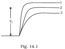
(a) 1 and 3 both correspond to forward bias of junction
(b) 3 corresponds to forward bias of junction and 1 corresponds to reverse bias of junction
(c) 1 corresponds to forward bias and 3 corresponds to reverse bias of junction.
(d) 3 and 1 both correspond to reverse bias of junction. - In Fig. 14.2, assuming the diodes to be ideal,
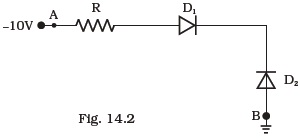
(a) D1 is forward biased and D2 is reverse biased and hence current flows from A to B
(b) D2 is forward biased and D1 is reverse biased and hence no current flows from B to A and vice versa.
(c) D1and D2 are both forward biased and hence current flows from A to B.(d) D1 and D2 are both reverse biased and hence no current flows from A to B and vice versa. - A 220 V A.C. supply is connected between points A and B (Fig. 14.3). What will be the potential difference V across the capacitor?
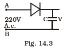
(a) 220V.
(b) 110V.
(c) 0V.
(d) 220 √2 V. - Hole is
(a) an anti-particle of electron.
(b) a vacancy created when an electron leaves a covalent bond.
(c) absence of free electrons.
(d) an artificially created particle. - The output of the given circuit in Fig. 14.4.
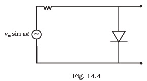
(a) would be zero at all times.
(b) would be like a half wave rectifier with positive cycles in output.
(c) would be like a half wave rectifier with negative cycles in output.
(d) would be like that of a full wave rectifier. - In the circuit shown in Fig. 14.5, if the diode forward voltage drop is 0.3 V, the voltage difference between A and B is
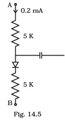
(a) 1.3 V
(b) 2.3 V
(c) 0
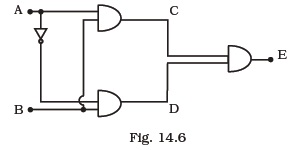
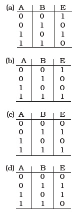
(d) 0.5 V - Truth table for the given circuit (Fig. 14.6) is
Multiple Choice Questions (MCQ II)
- When an electric field is applied across a semiconductor
(a) electrons move from lower energy level to higher energy level in the conduction band.
(b) electrons move from higher energy level to lower energy level in the conduction band.
(c) holes in the valence band move from higher energy level to lower energy level.
(d) holes in the valence band move from lower energy level to higher energy level. - Consider an npn transistor with its base-emitter junction forward biased and collector base junction reverse biased. Which of the following statements are true?.
(a) Electrons crossover from emitter to collector.
(b) Holes move from base to collector.
(c) Electrons move from emitter to base.
(d) Electrons from emitter move out of base without going to the collector. - Figure 14.7 shows the transfer characteristics of a base biased CE transistor. Which of the following statements are true?
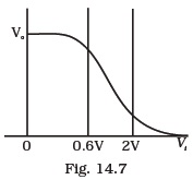
(a) At Vi = 0.4V, transistor is in active state.
(b) At Vi = 1V , it can be used as an amplifier.
(c) At Vi = 0..5V, it can be used as a switch turned off.
(d) At Vi = 2.5V, it can be used as a switch turned on. - In a npn transistor circuit, the collector current is 10mA. If 95 per cent of the electrons emitted reach the collector, which of the following statements are true?
(a) The emitter current will be 8 mA.
(b) The emitter current will be 10.53 mA.
(c) The base current will be 0.53 mA.
(d) The base current will be 2 mA. - In the depletion region of a diode
(a) there are no mobile charges
(b) equal number of holes and electrons exist, making the region neutral.
(c) recombination of holes and electrons has taken place.
(d) immobile charged ions exist. - What happens during regulation action of a Zener diode?
(a) The current in and voltage across the Zenor remains fixed.
(b) The current through the series Resistance (Rs) changes.
(c) The Zener resistance is constant.
(d) The resistance offered by the Zener changes. - To reduce the ripples in a rectifier circuit with capacitor filter
(a) RL should be increased.
(b) input frequency should be decreased.
(c) input frequency should be increased.
(d) capacitors with high capacitance should be used. - The breakdown in a reverse biased p–n junction diode is more likely to occur due to
(a) large velocity of the minority charge carriers if the doping concentration is small.
(b) large velocity of the minority charge carriers if the doping concentration is large.
(c) strong electric field in a depletion region if the doping concentration is small.
(d) strong electric field in the depletion region if the doping concentration is large.
Very Short Answer Type Questions
- Why are elemental dopants for Silicon or Germanium usually chosen from group XIII or group XV?
- Sn, C, and Si, Ge are all group XIV elements. Yet, Sn is a conductor, C is an insulator while Si and Ge are semiconductors. Why?
- Can the potential barrier across a p-n junction be measured by simply connecting a voltmeter across the junction?
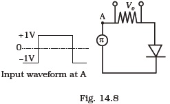
- Draw the output waveform across the resistor (Fig.14.8).
- The amplifiers X, Y and Z are connected in series. If the voltage gains of X, Y and Z are 10, 20 and 30, respectively and the input signal is 1 mV peak value, then what is the output signal voltage (peak value)
(i) if dc supply voltage is 10V?
(ii) if dc supply voltage is 5V? - In a CE transistor amplifier there is a current and voltage gain associated with the circuit. In other words there is a power gain. Considering power a measure of energy, does the circuit violate conservation of energy?
Short Answer Type Questions
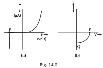
(i) Name the type of a diode whose characteristics are shown in Fig. 14.9 (A) and Fig. 14.9(B).
(ii) What does the point P in Fig. (A) represent?
(iii) What does the points P and Q in Fig. (B) represent?- Three photo diodes D1, D2 and D3 are made of semiconductors having band gaps of 2.5eV, 2eV and 3eV, respectively. Which ones will be able to detect light of wavelength 6000 Å?
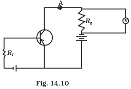
- If the resistance R1 is increased (Fig.14.10), how will the readings of the ammeter and voltmeter change?
- Two car garages have a common gate which needs to open automatically when a car enters either of the garages or cars enter both. Devise a circuit that resembles this situation using diodes for this situation.
- How would you set up a circuit to obtain NOT gate using a transistor?
- Explain why elemental semiconductor cannot be used to make visible LEDs.
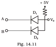
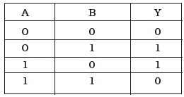
- Write the truth table for the circuit shown in Fig.14.11. Name the gate that the circuit resembles.
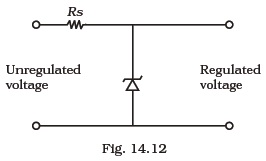
- A Zener of power rating 1 W is to be used as a voltage regulator. If zener has a breakdown of 5V and it has to regulate voltage which fluctuated between 3V and 7V, what should be the value of Rs for safe operation (Fig.14.12)?
Long Answer Type Questions
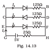
- If each diode in Fig. 14.13 has a forward bias resistance of 25Ω and infinite resistance in reverse bias, what will be the values of the current I1, I2, I3 and I4?
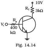
- In the circuit shown in Fig.14.14, when the input voltage of the base resistance is 10V, Vbe is zero and Vce is also zero. Find the values of Ib, Ic and β.
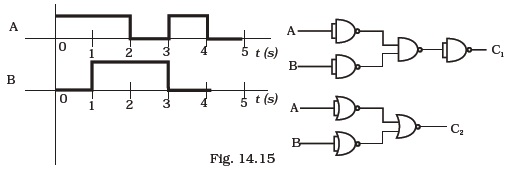
- Draw the output signals C1 and C2 in the given combination of gates (Fig. 14.15).
- Consider the circuit arrangement shown in Fig 14.16 (a) for studying input and output characteristics of npn transistor in CE configuration.
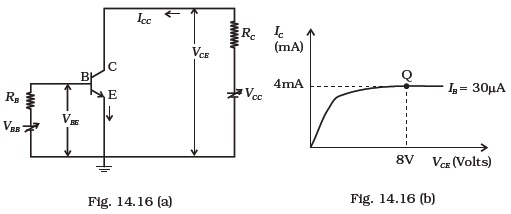
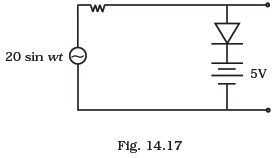
Select the values of RB and RC for a transistor whose VBE = 0.7 V, so that the transistor is operating at point Q as shown in the characteristics shown in Fig. 14.16 (b). Given that the input impedance of the transistor is very small and VCC = VBB = 16 V, also find the voltage gain and power gain of circuit making appropriate assumptions. - Assuming the ideal diode, draw the output waveform for the circuit given in Fig. 14.17. Explain the waveform.
- Suppose a ‘n’-type wafer is created by doping Si crystal having 5 × 1028 atoms/m3 with 1 ppm concentration of As. On the surface 200 ppm Boron is added to create ‘P’ region in this wafer.
Considering ni = 1.5 × 10¹⁶ m–3,
(i) Calculate the densities of the charge carriers in the n & p regions.
(ii) Comment which charge carriers would contribute largely for the reverse saturation current when diode is reverse biased. - An X-OR gate has following truth table:
It is represented by following logic relation
Y = A.B + A.B
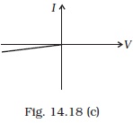
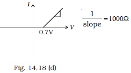
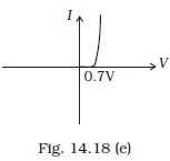
Build this gate using AND, OR and NOT gates. - Consider a box with three terminals on top of it as shown in Fig.14.18 (a):
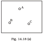
Three components namely, two germanium diodes and one resistor are connected across these three terminals in some arrangement. A student performs an experiment in which any two of these three terminals are connected in the circuit shown in Fig. 14.18 (b).
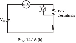
The student obtains graphs of current-voltage characteristics for unknown combination of components between the two terminals connected in the circuit.
The graphs are
(i) when A is positive and B is negative
(ii) when A is negative and B is positive
(iii) When B is negative and C is positive
(iv) When B is positive and C is negative
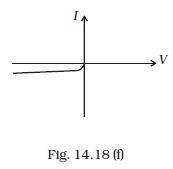
(v) When A is positive and C is negative
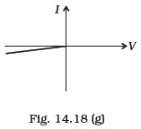
(vi) When A is negative and C is positive
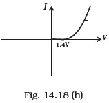
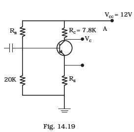
From these graphs of current – voltage characteristic shown in Fig. 14.18 (c) to (h), determine the arrangement of components between A, B and C. - For the transistor circuit shown in Fig.14.19, evaluate VE, RB, RE given IC = 1 mA, VCE = 3V, VBE = 0.5 V and VCC = 12 V, β = 100.
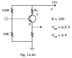
- In the circuit shown in Fig.14.20, find the value of RC.
| « Previous | Next » |
Answers to Multiple Choice Questions


Physics Chemistry Maths Biology
To get study material, exam alerts and news, join our Whatsapp Channel.